Pin Diagram For Ic 7483
Solved the diagram and results table for the 7483 adder is Adder bit ic 7483 using binary parallel adders four explain ques10 Ic adder bit 7483 binary using ques10 parallel joshi pooja description
Design and explain 8 bit binary adder using IC 7483.
Ic 7483 pin diagram, truth table, applications Pin on 3celectrons mall Adder bcd bit 7483 ic using explain example carry implementation
Design a 1 digit bcd adder using ic 7483 and explain the operation for
Design and explain 8 bit binary adder using ic 7483.Explain with example 4-bit bcd adder using ic- 7483. Adder bcd 7483 ic using digit circuit explain used outputIc 7483 pin diagram, truth table, applications.
Design and explain 8 bit binary adder using ic 7483.Truth applications etechnog Diagram logic ic 74ls08 chip 7408 7404 data gates gate datasheet pinout circuit connection choose board pdf seekic ib linda.


Pin on 3Celectrons Mall

Design and explain 8 bit binary adder using IC 7483.

Design a 1 digit BCD adder using IC 7483 and explain the operation for

Design and explain 8 bit binary adder using IC 7483.

Explain with Example 4-bit BCD adder using IC- 7483.

Solved The diagram and results table for the 7483 adder is | Chegg.com
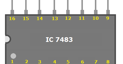
IC 7483 Pin Diagram, Truth Table, Applications - ETechnoG